6421 North Nirvana Place Tucson, AZ 85750 USA. Tel: 520.270.8086
E-mail : araca@aracainc.com
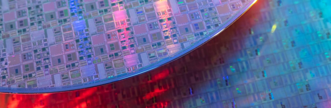
Founded in 2004 and headquartered in Tucson, AZ (USA), Araca Inc. provides unique, enabling, and fully customized solutions to our clients in the integrated circuit planarization and semiconductor polishing fields worldwide. Our clients include leading IC makers, consumables suppliers, OEMs, universities, and research centers. Our products provide you with the most non-intrusive way to lower the cost of ownership (COO) of your CMP or polishing modules. By working with us, you can save money and do your part in saving the environment by reducing slurry and rinse water consumption, increasing pad and diamond disc life, increasing polisher availability and throughput, and most importantly, increasing productivity and yield.
Flucto-CMP® and the Slurry Injection System (SIS®) are our flagship products. Compatible with all polishers, SIS® continues to be rapidly adopted in high-volume manufacturing due to its proven cost of ownership and environmental benefits. Flucto-CMP®, also compatible with all polishers, is currently being beta-tested at multiple OEMs, IC makers, and slurry suppliers. Furthermore, we provide sensorized and affordable state-of-the-art polishers-tribometers and PVA brush scrubbers-tribometers, for processing coupon-sized wafers all the way up to 300 mm. Our tools allow for significant reductions in process and consumables characterization costs, as well as research, and development expenses.
In our Class 100 clean room, we provide foundry services for substrates of all sizes and types (including wide-bandgap materials). When performing analytical and functional tests on pads, slurries, conditioners, retaining rings, brushes, and cleaning chemicals, we take pride in the quality and the scientific value of our work. Our confocal microscopy, pad surface preparation, pad grooving, and high-throughput pad dimensional QC services are second to none. We develop customized CMP, polishing, and cleaning consumables and processes for a variety of applications including SiC and GaN, and remain open to co-development programs. We also offer delayering services for 3D NAND and DRAM structures on coupon-sized wafers all the way up to 300 mm wafers.